- About Us

- Our Services
- Your Industry
- Resources
- News & Blog
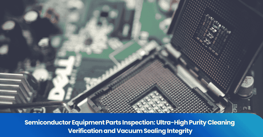
A single metallic particle smaller than a human hair can cause a batch of wafers worth tens of thousands of dollars to fail yield. A vacuum seal that leaks at 10⁻⁸ atm·cc/sec can destabilize an entire deposition process. Yet buyers sourcing semiconductor equipment parts — chamber components, gas delivery hardware, vacuum seals, fittings — from Chinese manufacturers routinely accept delivery on visual inspection alone. The cleanliness and hermetic integrity that define these parts cannot be seen with the naked eye, which is exactly why verification protocols exist.
This guide explains what ultra-high purity (UHP) cleaning verification and vacuum seal integrity testing involve, which standards apply, and how a third-party inspection on semiconductor equipment parts should be structured before a single component leaves the factory floor.
Key Takeaways
- UHP cleaning compliance is verified through particle count analysis, non-volatile residue (NVR) testing, and metal ion analysis — visual inspection is insufficient for any of these.
- Vacuum seal integrity requires helium mass spectrometry leak detection; the industry standard acceptable leak rate for fine leaks is typically ≤ 1 × 10⁻⁹ atm·cc/sec.
- SEMI F1, SEMI F19, SEMI F37, and ISO 14644-1 are the primary standards governing UHP component cleanliness and sealing requirements in semiconductor manufacturing contexts.
Why Semiconductor Equipment Parts Demand a Different Inspection Framework
Standard third-party inspection protocols — dimensional checks, visual defect assessment, functional testing — are designed for consumer and industrial products with visible failure modes. Semiconductor equipment parts operate in a completely different failure regime. The contamination that destroys a wafer batch is invisible. The leak that ruins a CVD process reads as a fraction of a nanogram of gas per second. A part can look immaculate and ship with metallic ion contamination at the parts-per-billion level that will directly impact device yield the moment it enters a process chamber.
Semiconductor fabrication occurs in environments classified under ISO 14644-1. Most critical processes take place in ISO Class 4 or Class 5 environments — that means fewer than 1,000 particles ≥0.1 µm per cubic meter of air. Chamber parts that have not been cleaned to UHP standards introduce their contamination burden directly into this environment, bypassing all cleanroom controls. The cost impact compounds quickly: a single contamination event during wafer fabrication can result in yield loss across an entire run.
The implication for buyers sourcing chamber components, vacuum hardware, gas delivery fittings, or subsystem assemblies from Chinese suppliers is straightforward: the inspection you need is analytical, not visual. TradeAider's pre-shipment inspection service can be configured with custom checklists to cover functional and analytical requirements for high-specification industrial components — including coordination with on-site or laboratory testing protocols.
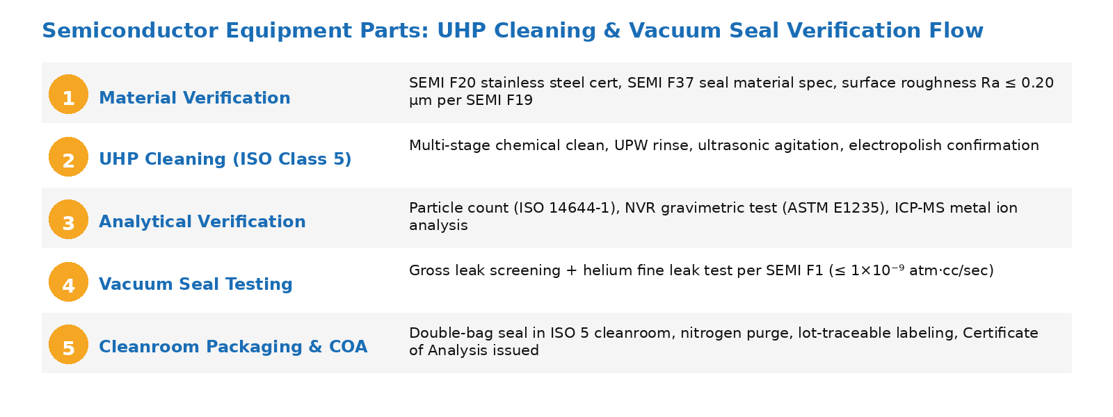
The five-stage verification sequence for semiconductor equipment parts: from material input through cleanroom packaging and COA issuance.
Part 1: Ultra-High Purity Cleaning Verification
What UHP Cleaning Means — and Why Factories Cut Corners
UHP cleaning for semiconductor parts goes significantly beyond industrial degreasing or standard precision cleaning. It typically involves multi-stage chemical processing: alkaline cleaning to remove organics, acid etching to remove metallic surface contamination, ultrasonic agitation in ultrapure water (UPW) to dislodge particles, followed by controlled drying and immediate cleanroom packaging. Surface finish requirements often mandate electropolishing to achieve a roughness average (Ra) of 8 µin (0.20 µm) or better, as specified in SEMI F19. The SC-01 Ultrahigh-Purity Process Specification from Swagelok, which guides production across the industry, covers both electropolished stainless steel and UHP plastic materials to these standards.
Chinese manufacturers producing semiconductor-grade parts vary enormously in their cleaning infrastructure. Tier-1 suppliers operate dedicated ISO 5 cleanrooms with HEPA or ULPA filtration and closed orbital welding equipment — environments where even manual TIG welding is prohibited because the arc releases metallic vapour into the air. Tier-2 and Tier-3 suppliers may claim UHP cleaning compliance while conducting final assembly in general manufacturing environments. Without analytical verification, there is no way to tell the difference at shipment.
The Three Analytical Tests That Verify UHP Cleaning Compliance
Three test categories form the core of UHP cleaning verification for semiconductor equipment parts:
| Test Type | What It Detects | Method | Relevant Standard |
|---|---|---|---|
| Particle Count Analysis | Residual particles by size and count on wetted surfaces | Liquid particle counter on rinse water or direct surface rinse | ISO 14644-1, SEMI E49.7 |
| Non-Volatile Residue (NVR) Testing | Organic residue remaining after solvent evaporation | Gravimetric analysis of evaporated rinse solvent | ASTM E1235, SEMI F20 |
| Metal Ion Analysis (ICP-MS) | Metallic contamination at parts-per-billion (ppb) levels | Inductively Coupled Plasma Mass Spectrometry on acid extract | SEMI F1, SEMI F37 |
Particle Removal Efficiency (PRE) testing — used to validate cleaning processes rather than individual parts — involves depositing known particle standards (such as NanoSilica or polystyrene latex particles) onto a surface, running the cleaning process, and measuring residual particle counts before and after. For buyers purchasing from manufacturers rather than evaluating cleaning equipment, the output they need is a Certificate of Analysis (COA) covering particle count, NVR, and ICP-MS results against agreed specifications for each batch.
Packaging verification is equally critical. Parts cleaned to UHP standards must be sealed in cleanroom conditions. An inspection should confirm that parts are double-bagged in certified cleanroom packaging, nitrogen-purged where specified, and that packaging integrity is intact at delivery. A COA without compliant packaging at the point of handover is a failed inspection.
What a Pre-Shipment Inspection for UHP Cleaning Should Confirm
A structured pre-shipment inspection for UHP semiconductor parts covers four checkpoints. First, the inspector verifies that cleaning was performed in the correct cleanroom classification — this means reviewing facility certification documentation and physically confirming that the final cleaning and packaging environment matches the claimed ISO class. Second, the inspector collects or witnesses collection of rinse samples for off-site particle count and NVR analysis — or reviews the manufacturer's test data against agreed acceptance criteria. Third, packaging integrity is checked on a representative sample: seal condition, labeling accuracy, cleanliness of outer packaging. Fourth, traceability documentation — lot numbers, material certifications, SEMI F20 compliance for stainless steel bar stock — is reviewed against the purchase order.
For high-volume procurement or critical applications, During production inspection can be deployed earlier in the manufacturing process to verify that material inputs (tube stock, fittings, seals) meet SEMI F20 and surface finish specifications before machining and assembly are complete — catching contamination risks at the point when they are still correctable.
Part 2: Vacuum Seal Integrity Verification
The Stakes of a Vacuum Seal Failure in Semiconductor Processing
Semiconductor manufacturing processes — CVD, PVD, ALD, etch, diffusion — take place under vacuum conditions ranging from rough vacuum (1–1,000 Pa) to ultra-high vacuum below 10⁻⁷ Pa depending on the process. Seals in these systems must maintain integrity under thermal cycling, chemical exposure, and repeated maintenance cycles. A vacuum seal failure introduces atmospheric gas and moisture into the process environment, disrupting deposition rates, contaminating chamber surfaces, and causing process instability that cannot always be traced back to the seal without significant diagnostic effort.
SEMI F1 establishes leak integrity requirements for high-purity vacuum systems — it is the foundational standard for acceptable leak rates in semiconductor gas distribution and vacuum applications. SEMI F37 covers elastomeric sealing material specifications for gas distribution systems, specifying outgassing behavior, chemical compatibility, and dimensional requirements. Together these standards define what a compliant vacuum seal must deliver, and they require quantitative leak rate testing — not visual inspection or pressure hold tests — to verify compliance.
Helium Leak Detection: the Industry Standard Method
Helium mass spectrometry leak detection is the standard method for fine leak testing in semiconductor vacuum components. Helium is used as the tracer gas because its small atomic size allows it to pass through the smallest possible leak paths, and mass spectrometers can detect helium at extremely low concentrations — the calibrated detection threshold is typically 10⁻⁹ atm·cc/sec, well below the leak rates that would cause process problems in service.
The test procedure involves pressurizing the part or assembly with pure helium (or placing it under helium atmosphere), then scanning with a mass spectrometer probe or placing it in a vacuum chamber connected to a spectrometer. Any helium escaping through a leak path is detected and quantified. For semiconductor chamber components, acceptable fine leak rates are typically ≤ 1 × 10⁻⁹ atm·cc/sec — a threshold that cannot be met or verified by any pressure decay or bubble-emission test method.
Gross leak testing (for larger, visible defects) is typically conducted by fluorocarbon liquid immersion per MIL-STD-883 method 1014 or equivalent, where a low-density liquid enters a leaking cavity and escapes visibly when the part is transferred to a high-density heated bath. Gross and fine leak tests are complementary — gross leak testing screens out severely defective parts cheaply before committing to the more resource-intensive helium fine leak test.
Vacuum Seal Inspection Checklist for Pre-Shipment Verification
| Inspection Point | Test Method | Acceptance Criterion |
|---|---|---|
| Seal face surface condition | Visual + surface profilometry | Ra ≤ spec per SEMI F19; no scratches, pitting, or tool marks |
| Elastomeric seal material | Material cert review + hardness test | FFKM or SEMI F37-compliant elastomer; correct shore hardness |
| Gross leak screening | Fluorocarbon liquid immersion or pressure decay | No bubble emission; pressure stable within spec |
| Fine leak rate | Helium mass spectrometry per SEMI F1 | ≤ 1 × 10⁻⁹ atm·cc/sec (or per purchase order spec) |
| Assembly torque records | Document review | Torque values per manufacturer's installation manual on file |
| Post-test packaging | Visual inspection of re-seal process | Re-packaged in cleanroom; no re-contamination of seal face |
One critical process point that many buyers overlook: helium leak testing introduces helium into the component under test. If re-packaging after testing is not performed inside a cleanroom environment by personnel in appropriate cleanroom garments, the testing process itself becomes a contamination event. This is why inspection standards and protocols for high-purity components must account for the environment in which inspection occurs — not just the test method.
Coordinating UHP and Seal Verification with Your Supplier Quality Agreement
The COA is the Starting Point — Not the Endpoint
A Certificate of Analysis is only as reliable as the testing laboratory that issued it and the chain of custody it represents. For buyers sourcing semiconductor parts from China, the practical risk is that a COA may be issued against a representative sample, a reference batch, or in some cases against an entirely different production lot. Third-party inspection closes this gap by independently witnessing or sampling from the actual production batch against which the COA is claimed.
The supplier quality agreement should specify: the ISO cleanroom class required for final cleaning and packaging; the analytical tests and acceptance limits for particle count, NVR, and metal ion contamination; the leak rate specification by component type; and the requirement for an independently witnessed or third-party-verified COA for each shipment lot. Buyers who embed these requirements in their purchase order terms rather than leaving them to factory discretion dramatically reduce the risk of receiving parts that will fail first-use qualification.
When to Deploy Pre-Production vs. Pre-Shipment Inspection
For new supplier relationships or first production runs of critical components, a pre-production inspection is the appropriate first step — verifying that the supplier's raw materials (stainless steel stock, seal materials, PFA tubing) meet the material specifications required by SEMI F20 and F37 before machining and cleaning investment is committed. Pre-shipment inspection then closes the loop at delivery, confirming that the finished, cleaned, tested, and packaged parts match what was specified and verified upstream.
For established suppliers with a track record, a well-structured pre-shipment inspection covering the checklist above — with real-time report access during the inspection — gives procurement and quality teams the visibility they need before approving a shipment that could cost significantly more to reject at their own facility than it would have cost to catch in China.
Frequently Asked Questions
What does "ultra-high purity" actually mean for semiconductor parts cleanliness?
Ultra-high purity cleaning achieves sub-ppb metallic ion contamination, particle counts below the thresholds defined by the applicable ISO 14644-1 cleanroom class, and NVR levels typically below 1 mg/0.1 m² of surface area. It requires dedicated cleanroom facilities, ultrapure water rinsing, and post-clean packaging inside the cleanroom — and must be verified analytically, not visually.
Why can't pressure decay testing replace helium leak testing for semiconductor vacuum seals?
Pressure decay testing is insufficiently sensitive for semiconductor vacuum applications. It can detect large leaks in the 10⁻³ to 10⁻⁵ atm·cc/sec range but cannot approach the 10⁻⁹ atm·cc/sec threshold required by SEMI F1 for high-purity vacuum systems. Helium mass spectrometry is required because helium's small atomic size and the mass spectrometer's selectivity allow detection at leak rates four to six orders of magnitude smaller than pressure decay methods can resolve.
How should buyers specify UHP cleaning requirements in a purchase order to a Chinese supplier?
Buyers should explicitly reference the applicable SEMI standards (F1, F19, F20, F37 as relevant), specify the required cleanroom class for final cleaning and packaging, state the analytical acceptance limits for particle count, NVR, and ICP-MS, require a witnessed or independently verified COA per production lot, and specify helium leak rate acceptance criteria by component type. Leaving any of these to "factory standard" exposes the buyer to compliance gaps that only appear at first-use qualification.
Can a third-party inspector in China perform helium leak testing on-site?
Helium mass spectrometry equipment is generally available through third-party testing laboratories in China's major manufacturing hubs. A pre-shipment inspection can be structured to include witness of helium leak testing at an accredited laboratory or, where the supplier has calibrated in-house equipment, witnessing the test at the factory with verification of calibration records. The inspector documents test conditions, calibration status, and results in real time — giving the buyer an independent record rather than relying solely on the supplier's own test report.
Conclusion
Semiconductor equipment parts are among the highest-consequence components a supply chain buyer can source from overseas — and among the least suitable for visual-only inspection. UHP cleaning compliance and vacuum seal integrity require analytical verification against defined standards, not a walk around the factory floor. Building these requirements into your supplier agreements and verifying them through a qualified third-party inspection before shipment is the only reliable way to protect your yield, your process qualification timeline, and your production schedule.
TradeAider's inspection team works with custom checklists for technically complex industrial components, with real-time report access during inspection and official documentation within 24 hours. Contact TradeAider to discuss a tailored inspection protocol for your semiconductor parts procurement, or use the Inspection Charge Calculator to estimate costs for your next shipment.
Related Articles
Grow your business with TradeAider Service
Click the button below to directly enter the TradeAider Service System. The simple steps from booking and payment to receiving reports are easy to operate.