- About Us

- Our Services
- Your Industry
- Resources
- News & Blog
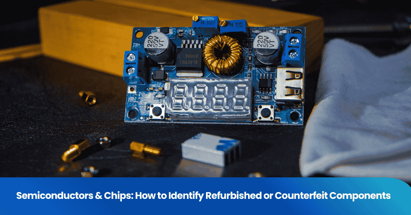
A counterfeit integrated circuit does not announce itself. It arrives in branded packaging, with a plausible date code, and often passes initial functionality testing — only to fail under thermal stress, voltage load, or after weeks of operation in the field. For buyers sourcing electronic assemblies or procuring components from Chinese manufacturers, the risk of receiving refurbished or counterfeit semiconductors is not theoretical. It is a documented, growing problem that has affected companies from consumer electronics OEMs to defense contractors. Understanding the specific types of counterfeit chips and the inspection methods that catch each type is the foundation of an effective incoming inspection program.
Key Takeaways
- Counterfeit semiconductors fall into distinct categories — recycled, remarked, subgrade, and cloned — and each requires a different detection method to reliably identify.
- Visual inspection alone catches only a fraction of counterfeit chips; electrical testing, X-ray analysis, and decapsulation are required for high-risk lots.
- Industry standards AS5553 and AS6081 provide structured frameworks for counterfeit avoidance and detection, applicable to both OEM procurement teams and independent distributors.
The Counterfeit Semiconductor Problem at Scale
What Is Driving the Risk
The global semiconductor supply chain has created structural conditions that favor counterfeit infiltration. Component shortages push buyers toward non-authorized distributors and brokers. Long product lifecycles mean systems continue to require parts long after original production has ended. And the sheer volume of electronic waste flowing through informal recycling channels in Asia provides an abundant raw material for refurbishment operations.
The Semiconductor Industry Association has estimated that counterfeit electronic parts cost manufacturers more than $7.5 billion annually. Field failures cost approximately ten times more to remediate than factory-stage failures — meaning a counterfeit component that passes initial inspection but fails in a deployed product triggers costs that compound at every step of recall, diagnosis, and replacement.
In 2022, ERAI reported a 35% increase in reported counterfeit parts compared to 2021, even as global semiconductor sales remained essentially flat. A 2011 U.S. Senate Armed Services Committee investigation identified over a million suspected counterfeit parts across 1,800 cases in defense supply chains. The U.S. Department of Defense estimates that as much as 15% of all spare and replacement parts for military electronics are counterfeit — and commercial supply chains, which lack the DoD's inspection infrastructure, face comparable or higher exposure.
A Taxonomy of Counterfeit Chip Types
Not all counterfeit semiconductors are created the same way, and understanding the specific type of counterfeit being encountered determines which inspection methods will catch it. The SAE AS5553 standard framework identifies five primary counterfeit types. For practical incoming inspection purposes, four categories cover the vast majority of encounters:
Recycled (reclaimed): Components harvested from scrapped circuit boards, cleaned, re-tinned, and repackaged as new. These are the most common counterfeit type. They carry genuine die from genuine manufacturers — but the die has already been through operating life, soldering cycles, and potentially thermal or electrical stress. Physical evidence includes oxidized or re-tinned leads, residual solder on pin bases, surface abrasion from removal, and mold compound contamination.
Remarked: Genuine components that have had their surface markings removed and replaced with different markings — usually to elevate apparent grade (commercial → industrial → military), speed grade, or manufacturer identity. Blacktopping — applying a thin coating of black material over the original surface before laser-marking new specifications — is the dominant remarking technique.
Subgrade / out-of-spec: Components that failed manufacturer testing at the wafer or package stage but were diverted to the gray market rather than destroyed. These carry genuine die and correct markings but do not meet the performance specifications on the label. They often pass room-temperature functional tests but fail under temperature extremes, high-frequency operation, or extended runtime.
Cloned: Counterfeit packages manufactured specifically to impersonate a genuine device. The die inside is fabricated by a different manufacturer (or a different process node) and does not replicate the genuine device's circuit architecture. Cloned parts often pass casual visual inspection but fail electrical parameter testing.
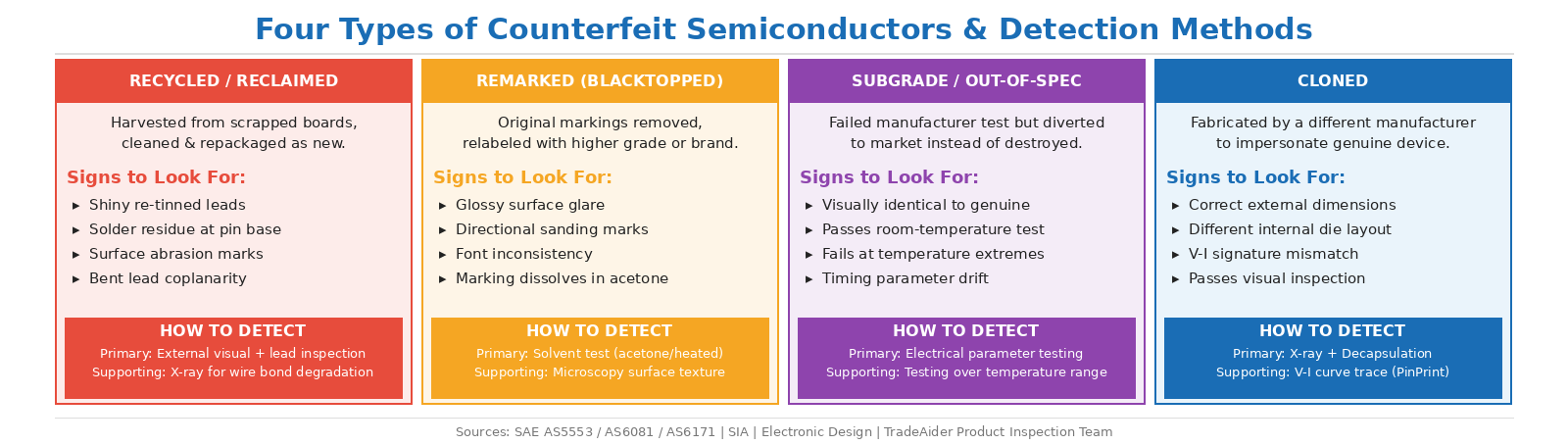
Four counterfeit semiconductor types and the primary inspection method most effective for detecting each.
Visual Inspection: The First and Fastest Screen
External Visual Inspection Checklist
External visual inspection under magnification (10×–40× stereo microscope) is the starting point of any incoming inspection protocol. It is not sufficient on its own for high-risk lots, but it eliminates a meaningful fraction of counterfeits at low cost and catches the most obvious cases of recycled and remarked parts.
The following physical indicators are the most reliable visual signatures of counterfeit or refurbished semiconductors:
Mold cavity cleanliness: Most plastic ICs have small cavities created intentionally during the mold process — pin-one markers, alignment features, or process artifacts. Counterfeiters have great difficulty keeping these cavities clean and consistent during their refinishing process, making contaminated or abnormally filled mold cavities one of the most reliable indicators of package surface reworking.
Surface texture and glare: An authentic component surface fresh from the mold has a consistent, non-reflective texture. A blacktopped surface has a higher, more uniform glare. Under a side-lit microscope, blacktopping appears as a fine layer that is slightly different in texture from the underlying substrate. Directional surface marks — parallel scratches from sanding — indicate that the original surface was ground to remove markings before re-coating.
Marking quality: Genuine chips carry clear, well-aligned, machine-applied text that is difficult to erase. Counterfeit chips often show jagged or blurry text, uneven character spacing, or markings applied using older silk-screen methods that leave a texture difference on the surface. Date codes that are impossible for the claimed manufacturer (e.g., a week-year code before the product was released) are immediate flags.
Lead condition: Authentic IC leads have a uniform, typically matte finish consistent with their lead-free or tin-lead surface treatment. Recycled components show excessively shiny leads from re-tinning over oxidized surfaces, residual solder at pin bases from board removal, or coplanarity deviation from mechanical extraction. A chip that has been ground down to remove original markings will often be measurably thinner than the OCM nominal thickness, and may have sharper package edges than the rounded profile of a correctly molded part.
Lot and date code consistency: Across the sampled units in a batch, date codes, lot codes, and manufacturer markings should be consistent. Mixed date codes within a single reel, or markings that vary in font weight or character sizing across units, indicate that parts from different sources have been combined and repackaged as a uniform lot.
Packaging and Documentation Review
Before physical inspection of the components themselves, the incoming documentation and packaging provide a first layer of verification:
Compare the part number, manufacturer, date code, and country of origin on the reel or tube label against the original purchase order and the manufacturer's part marking specification. Moisture-sensitive devices (MSDs) require dry-pack packaging with a humidity indicator card; counterfeiters frequently ship MSD parts without proper moisture barrier bags or with humidity indicator cards that show already-exceeded exposure. Certificate of Conformance (CoC) documents should be verified against OCM records where accessible.
Advanced Detection Methods by Counterfeit Type
Solvent Testing for Remarked Parts
For parts suspected of blacktopping or surface remarking, solvent testing provides a rapid, low-cost confirmation. The initial test applies acetone to the marking surface; many blacktopping materials dissolve with acetone, exposing original markings or a bare, polished substrate underneath. When remarking does not dissolve with acetone, more aggressive heated solvent analysis using chemicals at elevated temperatures can reveal tampering that basic acetone testing misses. This step screens specifically for remarked parts and takes minutes per sample.
X-Ray Signature Analysis
Non-destructive X-ray imaging is the most powerful intermediate-level inspection tool for semiconductor authentication. X-ray reveals the internal die frame design, die size and position, wire bond count and routing, and the overall internal architecture — none of which is visible from outside the package.
Authentic devices show consistent bonding wire diameters (typically 25–50 μm) and precise die alignment; X-ray systems verified against manufacturer blueprints can flag deviations in wire bond pattern and die positioning. Advanced X-ray software adapted from facial recognition algorithms compares internal structure measurements against a known-good "golden sample" to identify deviations automatically.
X-ray is particularly effective for detecting recycled components — wire bond degradation, broken bonds repaired with additional bonding material, and die paddle designs that don't match the OCM's standard construction are all visible. It also identifies cloned parts where the internal die architecture differs structurally from the genuine device. The most effective internal inspection protocol combines decapsulation of at least one unit to confirm die authenticity, then X-ray inspection of a larger sample from the same lot to confirm consistency across the batch.
Decapsulation
Decapsulation — chemically removing the encapsulation compound to expose the silicon die — provides the highest-confidence authentication for suspect semiconductors. With the die exposed, inspectors verify the die markings (manufacturer logo, part number, copyright notice, and mask revision are typically present on legitimate dies), circuit layout patterns, and construction features against known-good samples or OCM documentation.
Because decapsulation is destructive, it is applied to a sample — typically one or a small number of units from a lot — not to the entire batch. The units sacrificed for decapsulation are selected from within the AQL sample, and X-ray inspection of the remaining sampled units provides assurance that the lot is internally consistent. A die that matches the OCM's design, combined with X-ray confirmation of consistent internal architecture across the sample, provides high confidence in lot authenticity.
Electrical Testing: Catching Subgrade and Cloned Parts
Visual inspection and X-ray do not reliably detect subgrade parts — those with genuine die that simply don't meet their labeled specifications. Detecting subgrade parts requires electrical testing against the device's datasheet parameters.
For functional testing, the key electrical parameters to verify include: DC electrical parameters (supply current, output voltage levels, leakage currents); speed parameters (propagation delay, rise/fall times for logic devices); and where accessible, parametric behavior over temperature. Subgrade parts often pass room-temperature DC testing but fail timing or functional testing at temperature extremes, which is why AS6171 recommends testing electrical components over the operating temperature range as an optional but strongly recommended additional test for elevated risk levels.
Detection Method Selection by Counterfeit Type
| Counterfeit Type | Primary Detection | Supporting Test | Visual Alone Reliable? |
|---|---|---|---|
| Recycled / Reclaimed | External visual + lead inspection | X-ray for internal degradation | Partially — obvious cases only |
| Remarked (blacktopped) | Solvent test (acetone / heated) | Surface texture microscopy | Sometimes, for crude remarking |
| Subgrade / Out-of-spec | Electrical parameter testing | Testing over temperature range | No — visually identical to genuine |
| Cloned | X-ray + decapsulation | V-I curve trace / PinPrint | No — sophisticated fakes match external dimensions |
| Empty package (no die) | X-ray (no die visible) or basic electrical test | Weight measurement (underweight) | No — packaging may appear normal |
Standards Framework: AS5553, AS6081, and AS6171
Which Standard Applies to Your Organization
Three SAE International standards form the primary framework for counterfeit electronic component mitigation, each targeting a different point in the supply chain.
AS5553 applies to OEMs and organizations that design and manufacture products incorporating electronic components. It provides requirements for building counterfeit mitigation into procurement, design, and supplier management processes. AS5553 is particularly useful for organizations that design and manufacture products and need guidance on avoiding counterfeit components from inclusion in products. The most recent revision, AS5553E, was published in November 2025.
AS6081 is the complementary standard for independent distributors — companies that procure electronic parts from the open market rather than from authorized distribution channels. AS6081 requires detailed test and inspection methodology documentation including results, sample size, acceptance/rejection criteria, disposition, and which recognized industry standard test or inspection methods were used to ensure substandard parts are not overlooked. Even when not contractually required, procurement teams increasingly use AS6081 as a benchmark for evaluating supplier inspection capabilities.
AS6171 provides detailed risk-based testing instructions and prescribes specific test methods for different risk levels. AS6171 was introduced in 2016 and incorporates advanced methods including X-ray and electrical testing; AS6081A (2023) now points to AS6171 as the required standard for counterfeit mitigation testing. The minimum required testing level under AS6171 is Moderate Risk Level 2, which requires both external and internal physical inspection of the component.
Applying the Framework to Commercial Procurement
These standards originated in aerospace and defense but their principles are directly applicable to any electronics buyer sourcing from China or from non-authorized distribution channels. The practical questions these standards answer for a commercial buyer are: What documentation should I require from my supplier? What sample size should I inspect? What tests should I run for the risk level of this component? And what do I do when I find a suspect or confirmed counterfeit?
For components sourced from authorized OCM distributors with full traceability, the standard incoming inspection requirement is documentation verification and external visual inspection. For components sourced from brokers, gray market channels, or non-authorized distributors — which includes most open-market procurement in China — AS6081 Moderate Risk Level 2 testing applies: external visual inspection, documentation verification, and electrical parameter testing at minimum, with X-ray recommended for critical components.
The Role of Third-Party Inspection in Component Authentication
For buyers who cannot execute X-ray, decapsulation, or parametric electrical testing in-house, third-party inspection and testing services provide the capability without requiring capital investment in laboratory equipment. A third-party inspection at the factory or at a certified testing laboratory executes the incoming inspection protocol against the lot before any components are assembled or shipped.
This is particularly relevant when sourcing assembled electronic products from Chinese manufacturers, where the manufacturer may source semiconductors independently from their own supplier network. TradeAider's product testing services for electrical and electronic categories can be coordinated with pre-shipment inspection to verify both the assembly quality and the authenticity of key components before goods leave the factory.
For buyers evaluating a new supplier for the first time, a factory audit that includes assessment of the supplier's own incoming inspection capability for electronic components provides a structural quality assurance layer — verifying that the factory itself has appropriate counterfeit mitigation processes before any production begins.
The earlier in the supply chain a counterfeit component is detected, the lower the cost of resolution. At incoming inspection, a rejected lot is a supplier conversation. After assembly and shipment, the same discovery is a product recall. Contact TradeAider to discuss a testing and inspection plan appropriate for your next electronic component or product shipment from China.
Frequently Asked Questions
What is the difference between a recycled and a remarked counterfeit semiconductor?
A recycled (reclaimed) counterfeit is a used component that has been harvested from a scrapped circuit board, re-tinned, and repackaged as new. The die inside is genuine but has already accumulated operating life. A remarked counterfeit is a genuine component — which may be new or recycled — that has had its surface markings removed and replaced with different markings, typically to make a lower-grade or lower-speed device appear to be a higher-specification part. Both types can carry the same part number on their package, but they require different inspection methods: visual and lead inspection for recycled parts; solvent testing and microscopy for remarked parts.
Can visual inspection alone confirm that a semiconductor is genuine?
Visual inspection can rule out obvious counterfeits — crude remarking, grossly damaged leads, impossible date codes, or blacktopping with poor-quality materials that is visible under a microscope. However, sophisticated counterfeits pass external visual inspection routinely. Subgrade parts (genuine die that don't meet labeled specs) are virtually indistinguishable visually from legitimate parts. High-quality remarking is difficult to detect without solvent testing. Cloned parts with correct external dimensions and markings require X-ray or electrical testing to identify. For anything other than low-risk, low-value components from fully trusted sources, visual inspection alone is insufficient.
What is AS6081 and when does it apply to component procurement?
AS6081 is an SAE International standard specifying counterfeit avoidance requirements for independent distributors and organizations procuring electronic parts from the open market rather than from authorized OCM distribution. It applies whenever components are sourced from brokers, gray-market channels, or non-authorized suppliers. The standard requires documented test and inspection methodology, defined sample sizes, acceptance/rejection criteria, and procedures for handling suspect parts. The 2023 revision (AS6081A) points to AS6171 for specific test method requirements. While originally developed for aerospace and defense, AS6081 is increasingly adopted by commercial OEMs and electronics buyers as a best-practice benchmark for any procurement outside authorized channels.
Related Articles

Grow your business with TradeAider Service
Click the button below to directly enter the TradeAider Service System. The simple steps from booking and payment to receiving reports are easy to operate.