- About Us

- Our Services
- Your Industry
- Resources
- News & Blog
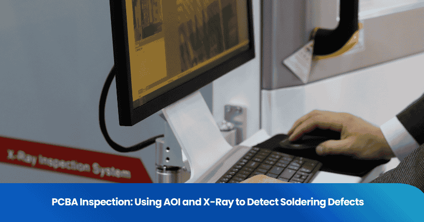
A solder bridge connecting two adjacent pads on a densely packed PCB. A void trapped beneath a BGA ball, silently degrading thermal performance. A head-in-pillow defect where the solder never fully fused—visible only in cross-section. These are the kinds of defects that escape visual inspection, pass through factory QC, reach the customer, and then fail in the field. For global buyers sourcing consumer electronics, smart home devices, or any product built around a PCB, understanding which inspection technology catches which defects—and at what cost—directly affects the risk profile of every order. This guide explains how AOI (Automated Optical Inspection) and AXI (Automated X-ray Inspection) work, what each is designed to catch, where they're positioned in the production process, and how buyers should interpret factory claims about PCBA inspection capability.
Key Takeaways
- AOI uses cameras and multi-angle lighting to detect surface-visible defects—solder bridges, missing components, misalignment, polarity errors—quickly and cost-effectively.
- X-ray inspection (AXI) is the only reliable method for hidden solder joint defects, particularly under BGA, QFN, and CSP packages where no camera can see.
- Post-reflow is the highest-value AOI placement—most assembly defects originate in the soldering process, making this the point of maximum defect density.
- Solder voids exceeding 25% of joint area are a reliability concern under IPC-A-610 standards; only AXI can measure and classify void percentages without destructive testing.
- AOI and AXI are complementary, not interchangeable—a PCBA with both represents a more robust inspection regime than either tool alone.
Why PCBA Soldering Defects Are Hard to Catch Visually
The Density Problem
A modern consumer electronics PCB—say, the main board of a wireless speaker or a smart plug—may contain 500 to 2,000 individual solder joints in an area smaller than a business card. Component packages like 0402 resistors (1.0 mm × 0.5 mm) and 01005 passives (0.4 mm × 0.2 mm) create solder joints that are invisible to the naked eye at normal inspection distances. Human visual inspection at this scale is not just slow—it's statistically unreliable. One study published in the International Journal of Engineering and Advanced Technology found that AOI reduces defect escape rates by up to 90% compared to manual inspection. The same research noted the cost-of-quality implication: fixing a defect in a bare board costs approximately 10 times less than fixing it in a fully assembled board, and roughly 1,000 times less than a field-deployed product.
The Hidden Joint Problem
Beyond density, modern component packaging creates a category of defects that no camera—no matter how high its resolution—can detect: joints hidden beneath the component body. Ball Grid Array (BGA) components place their solder connections underneath the package, with no line-of-sight from above. Quad Flat No-lead (QFN) packages and chip-scale packages (CSPs) have the same issue. AXI is the only practical inspection method for these hidden connections—it can see through the component body, image the solder joints beneath, and detect voiding within joints that would otherwise appear perfectly acceptable from the outside.
AOI: What It Does and Where It Works Best
How AOI Works on a PCBA
Automated Optical Inspection systems use high-resolution cameras, multi-angle programmable illumination, and image-processing software to scan a PCBA and compare it against a reference model—either a golden board or a CAD-imported template. The illumination system is purpose-built for solder joint analysis: RGB ring lights at multiple angles extract color information from solder surfaces. In a correctly formed joint, the flat top of the fillet reflects red light strongly; the rising slope of the solder climbing the component lead reflects green; the steeper slope reflects blue. By analyzing the ratio of red, green, and blue in each solder joint area and comparing it to the reference profile, the AOI system determines whether the joint geometry falls within tolerance or represents a defect. This is how 2D AOI distinguishes between a properly wetted joint and a cold joint, an insufficient solder condition, or a solder bridge—all based on optical properties rather than electrical testing.
Defects AOI Can Reliably Detect
In PCBA inspection, AOI excels at surface-visible defect categories. Solder bridges—where excess solder connects two adjacent pads or leads—appear as color anomalies in AOI images and are among the most reliably detected defect types. Missing components, where a pad location has no component placed, are detected by comparing the expected component silhouette against the actual image. Component misalignment and polarity errors (a diode or tantalum capacitor installed backwards) are caught by comparing expected orientation markers against actual placement. Tombstoning—where one end of a passive component lifts off the pad during reflow—is detected as geometric deviation. Insufficient solder and excess solder conditions are evaluated by solder area and height measurements. For buyers reviewing factory inspection capability, a well-programmed AOI system running at post-reflow represents a meaningful quality gate for these surface defects.
Where AOI Is Placed in the Production Flow
AOI can be positioned at multiple points in the SMT assembly process, but post-reflow is the most common and cost-effective placement because the majority of assembly defects originate during soldering. Some factories run pre-reflow AOI as well—after component placement but before the reflow oven—to catch placement errors before the solder is set, making corrections less costly. Sophisticated production lines may also run Solder Paste Inspection (SPI) before component placement, checking paste deposition volume and alignment before any components are placed. For buyers auditing a factory's PCBA inspection capabilities, the minimum expectation is post-reflow AOI. Pre-reflow AOI and SPI represent a more mature quality system and should be expected from suppliers producing complex, multi-layer designs.
AOI's Limitations: What It Cannot See
AOI's fundamental limitation is that it evaluates solder quality based on surface geometry and optical properties—it cannot assess internal joint structure. Voids trapped within a solder joint may be invisible from above. Cold joints that passed the reflow oven at marginally insufficient temperature may look acceptable in a 2D optical image while having poor internal wetting. Most critically, all solder connections beneath BGA, QFN, and CSP packages are completely outside AOI's field of view. A factory that relies on AOI alone for a PCB containing BGA components has a systematic gap in its inspection regime—one that buyers can identify by asking the right questions during a factory audit or during a During Production Inspection.
AXI: What X-Ray Inspection Adds to PCBA Quality Control
How X-Ray Inspection Works
Automated X-ray Inspection operates on a different physical principle than AOI. X-rays pass through the PCBA; dense materials like solder absorb more radiation and appear darker in the resulting image, while less dense areas—such as voids, air pockets, or gaps—appear lighter. This contrast allows AXI systems to image the internal structure of solder joints, not just their surface appearance. Modern AXI systems achieve resolution down to 1 micrometer, enabling detection of fine-scale defects in BGA solder balls with diameters as small as 0.3 mm. 3D AXI (computed tomography) systems capture multiple 2D projection images at different angles and reconstruct a three-dimensional model of the joint, allowing precise measurement of void volume, ball geometry, and joint-to-pad contact quality.
BGA Defects: The Primary Application of AXI
BGA components are the primary driver of AXI adoption in consumer electronics manufacturing. With hundreds of solder balls hidden beneath the package, BGAs are used in the highest-complexity components—microprocessors, memory chips, RF modules, application processors. The defects that matter most in BGA assemblies are ones only AXI can reliably find. Solder bridges (two balls fused together) create shorts that cause immediate functional failures and show clearly as connected dark masses in an X-ray image. Open connections (a ball that failed to contact the PCB pad) appear as missing or separated dark spots. Solder voids—air pockets trapped within the joint during reflow—appear as bright spots within the dark solder mass; excessive voiding above 25% of joint area is a reliability concern under IPC-A-610 standards, impairing both thermal conductivity and mechanical strength. And the most subtle defect—head-in-pillow (HIP)—occurs when the BGA solder ball and the solder paste on the PCB pad fail to coalesce during reflow, leaving a weak or nonexistent bond that passes electrical test at room temperature but fails intermittently under thermal stress.
The Head-in-Pillow Defect: Why AXI Is Non-Negotiable for BGA Products
Head-in-pillow (HIP) defects deserve specific attention because they are one of the most costly defect types in consumer electronics—they routinely pass end-of-line functional testing and only manifest as field failures weeks or months into customer use. HIP defects occur when PCB warpage under thermal stress during reflow prevents the BGA ball and solder paste from making full contact. The ball and paste each form a skin oxide layer during the heating and cooling cycle, preventing full fusion. The resulting joint resembles a "head resting on a pillow"—visually indistinguishable from the outside, electrically intermittent, and mechanically weak. For products using application processors, wireless chipsets, or any complex BGA-mounted IC, a factory without AXI capability is systematically unable to detect this failure mode. Buyers sourcing products with BGA components should make AXI inspection a specific requirement in their quality agreement and verify its use during factory audits.
AOI vs. AXI: Choosing the Right Tool for Each Defect Type
| Defect Type | AOI | AXI (X-Ray) | Notes |
|---|---|---|---|
| Solder bridge (surface) | ✅ Excellent | ✅ Capable | AOI preferred for speed and cost |
| Missing component | ✅ Excellent | ⚠️ Partial | AOI more reliable for component presence/absence |
| Component polarity/orientation | ✅ Excellent | ⚠️ Limited | AOI reads orientation markings directly |
| Solder void (joint interior) | ❌ Cannot detect | ✅ Excellent | AXI measures void % for IPC-A-610 compliance |
| BGA solder bridge (under package) | ❌ Cannot detect | ✅ Excellent | AXI is the only practical method |
| BGA open connection | ❌ Cannot detect | ✅ Excellent | AXI shows missing/separated solder balls |
| Head-in-pillow (HIP) defect | ❌ Cannot detect | ✅ Best with 3D AXI | 3D CT imaging shows ball-pad separation clearly |
| Tombstone / component lift | ✅ Excellent | ✅ Capable | AOI preferred for throughput |
| Through-hole fill quality | ⚠️ Limited | ✅ Excellent | AXI can verify fill percentage in plated holes |
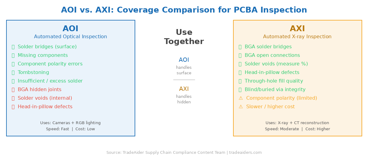
AOI covers surface-visible defects (left); AXI covers hidden solder joint defects beneath component packages (right)
What Buyers Should Ask When Auditing a Factory's PCBA Inspection Setup
Key Questions for AOI Capability
When evaluating a factory's AOI capability, the right questions go beyond "do you have an AOI machine?" Buyers should ask where AOI is positioned in the line (pre-reflow, post-reflow, or both); how often the AOI program is updated when new product designs or component changes are introduced; what the factory's process is for handling AOI-flagged boards (operator review, rework, re-inspection); and what their AOI false-positive rate is. A factory with a high false-positive rate either has poorly tuned AOI programs or inadequately trained operators—both of which mean the AOI is functioning as a bottleneck rather than a genuine quality gate. Request sample AOI reports from a recent production run for your product type; they should show defect images, defect classification, and board-level pass/fail data.
Key Questions for AXI Capability
For products containing BGA, QFN, or CSP components, AXI is not optional—it is the only way to verify hidden solder joint quality without destructive cross-sectioning. Buyers should ask whether the factory has an in-house AXI machine or subcontracts X-ray inspection; what percentage of boards receive X-ray inspection (100% inline AXI vs. periodic sample AXI); whether the system is 2D or 3D (3D AXI is significantly more capable for HIP and void measurement); and what the void acceptance criteria are and whether they align with IPC-A-610 standards. Factories that subcontract AXI or only apply it periodically to sample boards should be considered higher-risk for BGA-heavy assemblies. To understand how factories approach automated inspection more broadly, see What Is Automated Inspection and How Does It Work.
Connecting Factory Inspection to Third-Party QC
Why Factory AOI/AXI Records Matter for Your Pre-Shipment Inspection
A third-party Pre-Shipment Inspection of a PCBA-based product operates at a different level than in-line AOI or AXI. PSI inspectors conduct AQL-based sampling of finished, assembled units—they can perform functional tests, visual checks, and measurement checks, but they cannot run every board through an AOI or X-ray machine. This is why the factory's own AOI and AXI records are valuable inputs to a PSI. A well-designed Pre-Shipment Inspection for electronics should include review of the factory's IPQC records—AOI pass/fail rates per production run, AXI findings, First Article Inspection results—alongside the inspector's own sampling. When TradeAider's inspectors deliver their real-time report during a PSI, buyers can cross-reference factory QC data with independent findings to get a complete picture of production quality.
DPI for Electronics: Catching Process Problems at the Source
The most cost-effective intervention point for PCBA quality issues is during production—before the majority of boards are built. A During Production Inspection (DPI) for electronics focuses specifically on process quality: verifying that the factory's AOI is running and flagging boards correctly, that reflow oven profiles are within specification, that component lot changes are being handled with proper IQC steps, and that the IPQC team is responding to AOI findings with appropriate corrective action rather than simply reworking and re-passing boards. Buyers who have experienced PCBA quality failures often describe the same pattern: everything looked fine on the factory's self-reported QC data, but the underlying process was drifting and no one was escalating. DPI provides independent eyes on that process. For the broader context of how defects propagate through electronics production, see How Quality Defects Affect Product Safety and Reliability.
Frequently Asked Questions
Can AOI replace X-ray inspection for PCBA assemblies with BGA components?
No—AOI and X-ray inspection are complementary tools for distinct failure modes. AOI is optimized for surface-visible defects and operates fast enough for inline 100% inspection. AXI is the only method capable of imaging solder joints beneath BGA, QFN, and CSP packages, detecting voids within joints, and identifying head-in-pillow defects. A PCBA containing BGA components that is inspected by AOI only has a systematic gap: all hidden-joint defect modes are uninspected. For high-volume production of BGA-heavy assemblies, inline 3D AXI is the industry best practice for complete solder joint coverage.
What is a solder void and why does it matter?
A solder void is an air or gas pocket trapped inside a solder joint during the reflow soldering process. Voids form when volatile materials in the solder paste—flux residues, absorbed moisture, or organic contaminants—outgas during reflow and become trapped as the solder solidifies around them. Small voids are normal and acceptable; the IPC-A-610 standard becomes concerned when voids exceed 25% of joint area. Beyond that threshold, voids impair the joint's thermal conductivity (critical for power components), reduce mechanical strength, and can act as stress concentrators that accelerate fatigue cracking under thermal cycling. X-ray inspection measures void area precisely and can provide void percentages for each joint, enabling data-driven accept/reject decisions against your quality standard. Use TradeAider's AQL Calculator to plan your sampling approach for PCBA inspection.
What is a head-in-pillow (HIP) defect and why is it dangerous?
Head-in-pillow is a BGA solder joint defect where the solder ball and the solder paste deposit on the PCB pad fail to fully coalesce during reflow. Both surfaces form a thin oxide layer during the heating cycle that prevents fusion, leaving a joint where the ball appears to rest on top of the paste without bonding—like a head on a pillow. HIP defects are particularly dangerous because they often pass electrical continuity testing at room temperature, since the ball makes light physical contact with the pad. Under thermal cycling or mechanical stress in service, the contact fails, causing intermittent electrical failures that are difficult to diagnose. The primary cause is PCB or BGA package warpage under thermal stress during reflow. 3D AXI cross-sectional imaging is the most reliable way to detect HIP defects in production.
How should buyers verify a factory's AOI/AXI capability before placing an electronics order?
The most direct method is a factory audit that specifically evaluates the quality control equipment and processes. During an audit, inspectors can physically verify the presence and operational status of AOI and AXI machines, review recent PCBA inspection records, and assess whether the factory's QC team is trained to interpret and act on inspection results. Without a physical audit, buyers can request photo documentation of the inspection equipment and production line layout, plus sample AOI/AXI inspection reports from a recent production run for a comparable product. As an official Amazon SPN partner, TradeAider conducts factory audits that specifically assess supplier quality management systems—including inspection equipment and process compliance.
PCBA defects that escape factory inspection don't disappear—they become returns, negative reviews, and account health problems. TradeAider's During Production Inspection and Pre-Shipment Inspection services give you independent visibility into both process quality and finished goods quality, backed by real-time reporting and an official report within 24 hours. See how During Production Inspection works → or estimate your inspection cost for your next electronics order.
Related Articles


Grow your business with TradeAider Service
Click the button below to directly enter the TradeAider Service System. The simple steps from booking and payment to receiving reports are easy to operate.